Stencil is an art technique that illustrates an image by passing ink over a plate with holes. The semiconductor industry also has a similar technique. Stencil lithography is a method to pattern on a substrate by depositing metals through a shadow mask. The technology is normally used to make nano-sized devices or circuits; however, it is difficult to apply on curved surfaces.
The research team of Professor Seok Kim (ME), Prof. Dae Sung Chung (CE), and Ph.D. candidate Sangyeop Lee invented the shadow mask for stencil lithography that can be applied on flat and curved surfaces and can be attached and separated without any structural damage. The research was published as the front inside cover of Advanced Materials Technologies.
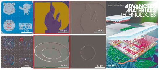
To proceed with the stencil lithography process on a curved surface, the shadow mask must be flexible and thin enough to make conformal contact on the curved shape. Currently, researchers are using masks made from organic materials, but storing and controlling them is tricky, and re-usage is unfavorable due to its fragility. In addition, previous research required additional structures to align the shadow mask, which limited substrate material selection and process scaling.
Furthermore, they made a dry adhesive with polydimethylsiloxane (PDMS) to attach a shadow mask on the substrate. The closer the distance between the mask and the substrate, the higher the resolution of the pattern appears. This adhesive allowed the mask to be easily attached and detached from the substrate like a clean Post-it note, and there was no damage done in the process.
The research team printed patterns clearly on curved substrates using their newly developed mask and adhesive. Also, they succeeded in multi-layer patterning, which stacks metals layer by layer, by using chromium (Cr) and titanium (Ti) metals and in manufacturing organic thin-film transistors (OTFTs) on both curved and flat substrates.
Prof. Kim, who led this research, said, “We have developed a shadow mask that achieves high resolution, curved surface compatibility, and multi-layer patterning,” and added, “The mask can be reused by cleaning it with an etchant even after multiple uses, so the potential is endless.”
This research was supported by the National Research Foundation of Korea (NRF) and the Ministry of Science and ICT.