Semiconductors have become indispensable in our daily lives. However, their continuous development has led to the problem of an increase in environmental costs. Lately, industrial and academic communities have struggled to cope with the inevitable production of greenhouse gases and waste. Currently, Metal oxide/polycrystalline silicon (LTPO) is the dominant semiconductor due to its long battery life, but its manufacturing process is costly and complicated. To meet the growing demands for environmental, social, and governance (ESG) management, continuous research to develop a more simple and environmentally friendly manufacturing process for semiconductors has been conducted.
A research team led by Professor Yong-Young Noh and Dr. Ao Liu (CE) has successfully developed a high-performance n-type semiconductor of Bi2S3 and p-type Te semiconductor using a simple thermal evaporation process. This production method attracted global attention due to its inexpensive and environmentally friendly nature along with its availability of being used to manufacture a variety of semiconductor circuits.
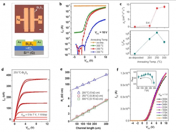
Prof. Noh’s team used the transition metal chalcogen: a transition metal added to sulfur, selenium, and tellurium. Instead of the conventional solution process, the research team used Bi2S3 to manufacture the thin film of the semiconductor through thermal evaporation in a high vacuum which leads to the resulting steam attaching to the board. Simple thermal treatment can control the quantity of electric charge, and semiconductors can be discretionally manufactured without doping.
If this transistor and electronic circuit manufacturing process are added to the standard manufacturing process for OLEDs, they may be manufactured through a
single-step process. This will significantly lower manufacturing costs, one of its biggest disadvantages. Also, current thermal evaporation equipment can be utilized which lowers the cost of the transition in manufacturing methods.
Prof. Noh noted, “Bi2S3 and Te used for this research are attractive materials that can be transitioned from conductors into semiconductors through a simple thermal treatment. This research will lead to additional studies using chalcogen semiconductor devices and commercialization of the related technology. We are planning to expand this research into memory devices and neuromorphic devices using this new development.”
The study, published in Nature Communications, was supported by the National Research Foundation of Korea and Samsung Display Corporation.