It may now be possible to make semiconductors through 3D printer printing process.
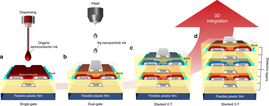
Through cooperation, professor Jung Sung-june (CiTE), Dr. Kwon Ji-min(CiTE Ph.D), professor Cho Kil-won(CE) research team, and professor Shizuo Tokito’s research team from Yamagata University has succeeded in implementing the world’s most integrated printed flexible semiconductor circuit by continuously stacking semiconductor devices printed on flexible plastic boards using 3D printing technology. They also improved the printed transistor’s performance by reducing its electric power consumption and amplifying maximum current.
Until now, there have been difficulties in commercializing organic semiconductors because of their large transistor size and low degree of integration. The research team focused on the fact that the low degree of aggregation was due to printing a single thin film transistor consisting of a single gate in a flat surface. So, for the first time in the world, they developed a two-way dual-gate transistor which is stacked in 3D to make various 3D digital logic circuits. This dual-gate element structure maximizes the performance of printed transistors and improves efficiency by making current flow twice as much than that of a single gate.
It is expected that by building electronic devices and circuits on top of plastic through these three-dimensional stacking techniques, semiconductor integration can be drastically increased, contributing to the commercialization of flexible electronic circuits that require a large number of transistors. Since it can be made in low-temperature conditions, its production cost is low. It can be used for wearable electronic devices quickly and easily so it is expected to help commercialize these kinds of fields.


